Transistor boost circuit for AE (Kurts Quad Boost)
Mar 6, 2021 13:12:41 GMT
admin, NightMachines, and 1 more like this
Post by keurslagerkurt on Mar 6, 2021 13:12:41 GMT
Hey all!
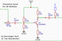
As promised, here is the schematic of my transistor boost. (Edit, for the intended boost, R3 needs to be 4.7K, not 47k. But the 47k also gives cool results. More info further down in another comment)

Its a very simple, emitter follower transistor circuit, inspired by the LPB-1 guitar boost pedal. I wanted to design this circuit as an exercise while I'm learning about transistors (reading 'the art of electronics'!), and I ended up liking the sound so much that I made a 1U PCB with four of these on it. A little bit of insight on how I went to design this:
- Took these values from the LPB-1 pedal: a bias voltage of 0.8V, and the quiescent current at the transistor base (don't have my calculations with me right now, don't remember the exact number).
- I calculated R4 and R3 with the quiescent current and with the design criterium that the emitter should be at 2.5V in steady state (ie so the waves are centered here, and the signal can go about 2.5V without clipping in both directions)
- I calculated R1 and R2 so the base is at 0.8V and the current through the divider is >10 times as large as the quiescent current.
- Calculated C1 and C2 so the high pass filter they form has a cutoff below audio rate
- placed R5 to be sure the outgoing wave is centered around 2.5V (but the circuit works pretty clean without it anyway)
So when I measured the circuit on the breadboard, all values where pretty close! Found about 0.8V at the base (a little bit more IIRC), found a bit less than 2.5V at the emitter. The cool thing about this circuit, is that it behaves very differently depending on the incoming signal volume. The circuit has a fixed amount of gain or boost, depending on the transistor you plop in, so you can control the amount of clipping with the input pot (I called it gain, but its actually a simple attenuater, forming a voltage divider with the input impedance of the circuit.) When you input a low volume signal, it works as a fairly clean boost, when you amp up the input, it first becomes a very crunchy boost with lots of high end. Amping the input even further, the circuit becomes more fuzzy, square wavey, and has a lot more low end and way less highs. I'm not exactly sure why this is, i know that transistors behave differently on low and high frequencies, so maybe that changes the cutoffs? Anyway, I really like it, cause you get some filter-y properties with this circuit that are fun to tweak and can also be voltage controlled by the use of a simple VCA in front!
I suggest anyone with a breadboard and a super standard NPN transistor to try it on the breadboard, its a lot of fun. I tried it with BC547, 2N5088 and 2n2222a, they all sounded great.
If anyone is interested in more detailed numbers or calculations, please ask, I have my notes somewhere here, so I can search them if there is interest. Also, all input, ideas, problems you see are ofcourse very welcome!
Cya!
Kurt
As promised, here is the schematic of my transistor boost. (Edit, for the intended boost, R3 needs to be 4.7K, not 47k. But the 47k also gives cool results. More info further down in another comment)

Its a very simple, emitter follower transistor circuit, inspired by the LPB-1 guitar boost pedal. I wanted to design this circuit as an exercise while I'm learning about transistors (reading 'the art of electronics'!), and I ended up liking the sound so much that I made a 1U PCB with four of these on it. A little bit of insight on how I went to design this:
- Took these values from the LPB-1 pedal: a bias voltage of 0.8V, and the quiescent current at the transistor base (don't have my calculations with me right now, don't remember the exact number).
- I calculated R4 and R3 with the quiescent current and with the design criterium that the emitter should be at 2.5V in steady state (ie so the waves are centered here, and the signal can go about 2.5V without clipping in both directions)
- I calculated R1 and R2 so the base is at 0.8V and the current through the divider is >10 times as large as the quiescent current.
- Calculated C1 and C2 so the high pass filter they form has a cutoff below audio rate
- placed R5 to be sure the outgoing wave is centered around 2.5V (but the circuit works pretty clean without it anyway)
So when I measured the circuit on the breadboard, all values where pretty close! Found about 0.8V at the base (a little bit more IIRC), found a bit less than 2.5V at the emitter. The cool thing about this circuit, is that it behaves very differently depending on the incoming signal volume. The circuit has a fixed amount of gain or boost, depending on the transistor you plop in, so you can control the amount of clipping with the input pot (I called it gain, but its actually a simple attenuater, forming a voltage divider with the input impedance of the circuit.) When you input a low volume signal, it works as a fairly clean boost, when you amp up the input, it first becomes a very crunchy boost with lots of high end. Amping the input even further, the circuit becomes more fuzzy, square wavey, and has a lot more low end and way less highs. I'm not exactly sure why this is, i know that transistors behave differently on low and high frequencies, so maybe that changes the cutoffs? Anyway, I really like it, cause you get some filter-y properties with this circuit that are fun to tweak and can also be voltage controlled by the use of a simple VCA in front!
I suggest anyone with a breadboard and a super standard NPN transistor to try it on the breadboard, its a lot of fun. I tried it with BC547, 2N5088 and 2n2222a, they all sounded great.
If anyone is interested in more detailed numbers or calculations, please ask, I have my notes somewhere here, so I can search them if there is interest. Also, all input, ideas, problems you see are ofcourse very welcome!
Cya!
Kurt


